Physical Address
304 North Cardinal St.
Dorchester Center, MA 02124
Physical Address
304 North Cardinal St.
Dorchester Center, MA 02124

Jon Peddie has been a graphics market analyst for about 35 years. We first met back when I was working on the TMS340 graphics processor family and the Video-DRAM (VRAM) in the mid-1980. Jon just published a retrospective article about the TMS34010 and VRAMs. I wanted to add some background information to his article and an old Byte Magazine article that gives some perspective as to the graphics accelerator board market of that era.
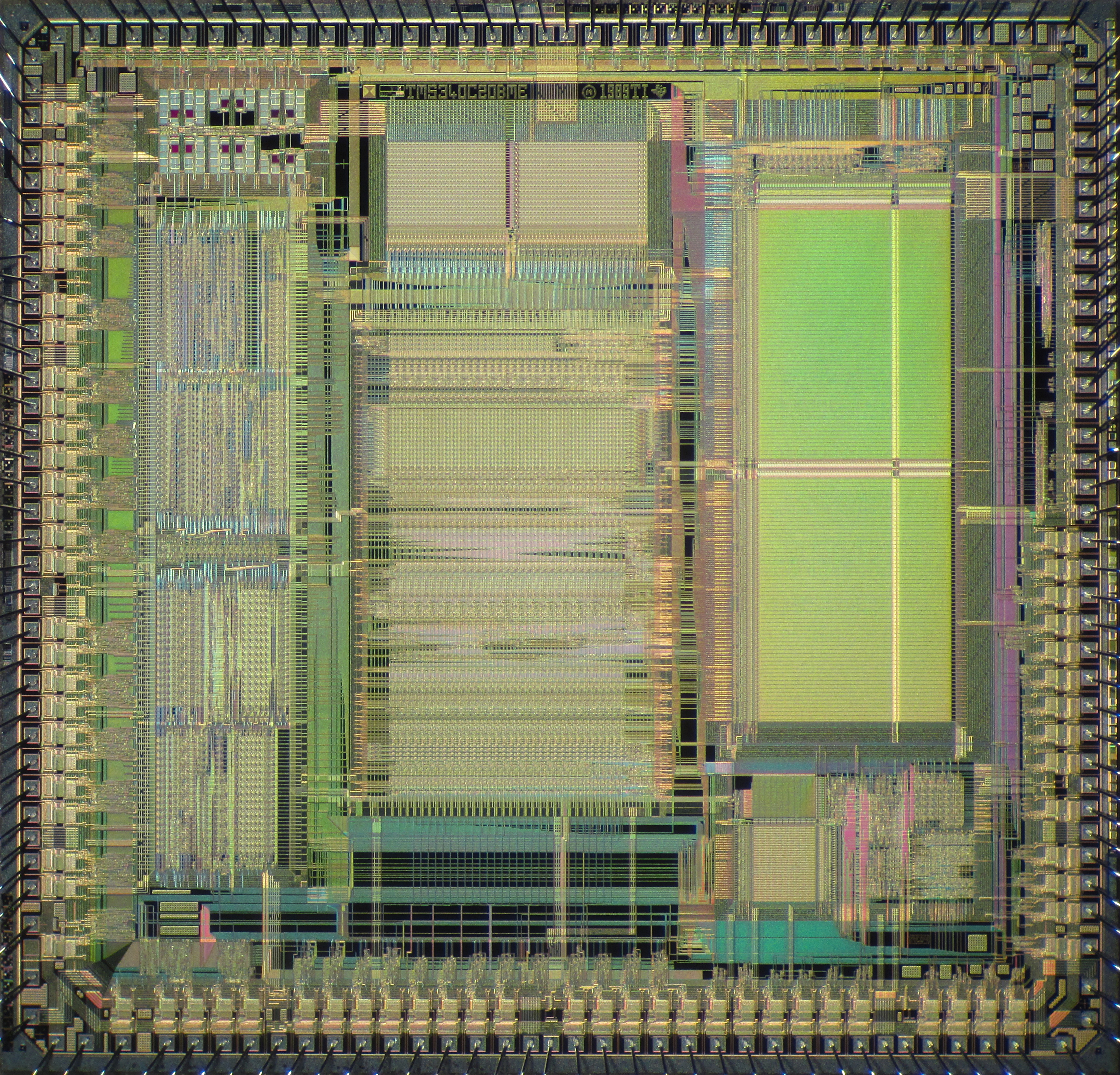
I have lived two somewhat different lives in high tech. My first 20 years were with Texas Instruments where I became the youngest TI Fellow in the history of the company. At TI, I worked on the architecture and logic design of the TMS9918 VDP (the first “Sprite Chip”), the TMS9995 and TMS99000 (16-bit microprocessors), the TMS34010 and TMS34020 (the first programmable graphics processors), and the TMS320C80 (image processor with, four VLIW DSPs and a RISC CPU on a chip).
The TMS9918 design started in 1977 was copied by the display chips used in the early Nintendo and Sega game systems and was the first consumer device interfacing directly with DRAMs. One of my first jobs was to figure out the timing to interface with DRAMs, which before the Synchronous DRAM (SDRAM) had very complex timing with over 30 critical timing parameters. The TMS34010 graphics processor was the first fully programmable processor to directly interface with DRAMs and the first processor to use the VRAM (a DRAM with a high-speed shift register and the precursor to today’s GDRAM and the SDRAM). The TMS320C80 was the first processor to directly interface with the Synchronous DRAM.
While we had to use DRAM to support the large memory demands of graphics processors, the bandwidth of DRAMs was becoming too slow to keep up with our needs. This caused me to work with TI’s memory division on the first practical VRAM in the early 1980s. My first-hand experience with the problems of interfacing to DRAMs and the work with VRAMs, in turn, led to my helping out TI’s Memory Group on the development of the Synchronous DRAM. In many ways, today’s SDRAM and GDRAM are direct descendants of the VRAM.
BTW, I make the distinction of the first “practical VRAM” because the idea of putting a shift register on a DRAM for supporting video display has multiple overlapping claims of invention including TI, IBM, and AT&T. What my team did was make a series of improvements to the basic concept to make it work in a system and help pushed the idea out into the market.
It so happens, I’m in the process of going through many thousands of pages of old articles about work I did back in my days at TI and I came across a November 1989 article, “The Brains Behind the Graphics” in Byte Magazine about graphics cards based on the TMS34010. I thought this reference would make a good companion to Jon Peddie’s retrospective.
While few today would know it, in the mid to late 1980s and early 1990s, before NVidia (founded 1993) and in the early days of ATI (founded 1985), the TMS34010 family dominated graphics cards used in Photoshshop® and CAD as discussed in the Byte article (see quote from the article below).
TI’s TMS34010 is probably the most popular graphics processor in the current PC market. Its powerful graphics capabilities have earned it a place in every thing from frame grabbers to printer
Byte Magazine Nov. 1989 “The Brains Behind the Graphics,” by Steve Apiki, Howard Eglowstein, and Rick Grehan
controllers, including, of course, display controllers.
I recently installed at NVidia Quadro P4000 board in my PC for doing some CAD work that costs about $750. I had forgotten how much graphics cards cost back in 1989 and was reminded by the article. Below is a table showing the various cards you could buy back then for doing Photoshop and CAD. The “Video Memory” was VRAM and the “Additional Memory” was either left over space in the VRAM or additional DRAM on the graphics card. The adjustment for inflation between 1989 and January 2019 is 2.03x, so double the prices below for comparison. Also note, we were talking in terms of one to two megabytes of memory back then and frame buffers were mostly 8-bits per pixel with a “color palette” (RAMDAC) to convert to red, green, and blue because memory was so expensive.

I’m heading to CES and my schedule is almost fully booked. I will be spending most of my time in the AR area of South Hall and in the Sands Expo along with some private meetings in the various hotels.


I would like to note that the TI99/4A had a shift register DRAM optimized for a block-glyph video VPU. (They used the term GRAM for it, and it consisted of most of their RAM). It was remarkably similar to the GDRAM and SGDRAM used shortly after your VRAM designs. (It had two separate shift registered ports if I recall, one for CPU side, one for VPU).
Of course, it would never be considered fast enough to be practical for any modern applications. In fact, the lack of speed was one of the two reasons to use a block glyph function instead of a full screen bitmap. (The other being price per a kilobyte.)
Thanks, but the function of GRAM was very different, and I think you may be misremembering some of the histories.
The way it worked was more like a very slow DMA access. I don’t know if you caught it, but I was one of six engineers on the TMS9918/28/29, the video processor for the 99/4A, and defined the DRAM interface on the 9918. I was also one of two people that worked out all the display memory accesses and how sprites worked.
The DRAM was only accessible by the TMS9918/28/29. A CPU got access to the DRAM (what the Home Computer called GRAM) to load up a starting address in the 9918. Then it would make requests for memory access to the 9918. The 9918 only had about 1 in 4 memory cycles free (depended on the graphics mode) where it could read or write to the DRAM 8-bits (1 byte) for the CPU. After accessing the DRAM, it would send a flag to the CPU that the data had been read or written and increment the address pointer. The CPU could then make a series of sequential accesses, but still, it took many cycles between each access. The CPU also had 256-bytes (not kilobytes but bytes) of RAM, and the GROM was a slow ROM with a similar DMA-like slow access.
The TMS9918 was the first consumer device to use DRAMs. We initially designed it for 4K (bit) DRAMs, but by the time it when to market in a big way, the 4Ks were being withdrawn from the market, and all the designs in production used 16K and above DRAMs. With the 16K DRAMs, we actually had plenty of memory for doing full bitmapped graphics. The problem was that the memory interface at the time was too slow. The 9918 only did full memory cycles and could not take advantage of “page mode,” which allowed faster sequential access, but the control and timing were very complicated. DRAMs had no clock back then, and everything had to be controlled with dozens of analog timed edges. You had to meet literally pages of timing relationships (I know because I worked through them for both the 9918 and 34010). Working through the timings made me advocate for the SDRAM, which I helped the TI’s DRAM group develop. Before the SDRAM, I was an advocate and helped define the Multiport DRAM with a separate serial port to support bitmapped video. Then there was the Multiport SDRAM that combined the SDRAM and Multiport VDRAM (also called VRAM). Finally, the GRAM is essentially an SDRAM with faster internal organization and banking to support random and serial access with a single I/O port.
Without page mode and complexity, which we could not afford at the time, there simply were not enough memory accesses to support a 4-bit per pixel bitmap. It was memory cycles and not the amount of memory that limited the 9918 and later 9918A and 9118. The best I could come up with later was the “graphics 2 mode,” which utilized more of the 16K DRAMs but was still limited by the memory access speed. The price of DRAM or the amount of it was not a problem with the 16K DRAMs.
Remember, this was 1977, and there were no PCs, and essentially only large mainframe computers and workstations talked to DRAM. Microprocessors only had SRAM interfaces. If you wanted to talk to DRAMs, you had analogy delay lines the could be tuned to optimize. For the consumer use of DRAM, we had to cobble together the interface with timing signals from our clock and some very simple delay lines.
The Multiport-DRAM (or VDRAM/VRAM but very different than the 9918’s ordinary DRAM, which was also called VRAM). Leveraged that a whole row of memory bits (256 on the first VDRAM) could be dumped into a shift register (or later an SRAM) broadside within the DRAM chip. Once the shift register was loaded, the bits could be shifted out for 256 cycles while the CPU was given full access for reading and writing.